- 您现在的位置:买卖IC网 > Sheet目录1993 > DS1305E/T&R (Maxim Integrated Products)IC RTC SERIAL ALARM 20-TSSOP
DS1305
4 of 22
PIN DESCRIPTION (continued)
PIN
DIP
TSSOP
NAME
FUNCTION
12
15
SDI
Serial Data Input. When SPI communication is selected, the SDI pin is the
serial data input for the SPI bus. When 3-wire communication is selected, this
pin must be tied to the SDO pin (the SDI and SDO pins function as a single I/O
pin when tied together).
13
16
SDO
Serial Data Output. When SPI communication is selected, the SDO pin is the
serial data output for the SPI bus. When 3-wire communication is selected, this
pin must be tied to the SDI pin (the SDI and SDO pins function as a single I/O
pin when tied together).
14
17
VCCIF
Interface Logic Power-Supply Input. The VCCIF pin allows the DS1305 to drive
SDO and
PF output pins to a level that is compatible with the interface logic,
thus allowing an easy interface to 3V logic in mixed supply systems. This pin is
physically connected to the source connection of the p-channel transistors in
the output buffers of the SDO and
PF pins.
15
18
PF
Active-Low Power-Fail Output. The
PF pin is used to indicate loss of the
primary power supply (VCC1). When VCC1 is less than VCC2 or is less than VBAT,
the
PF pin is driven low.
16
20
VCC1
Primary Power Supply. DC power is provided to the device on this pin.
OPERATION
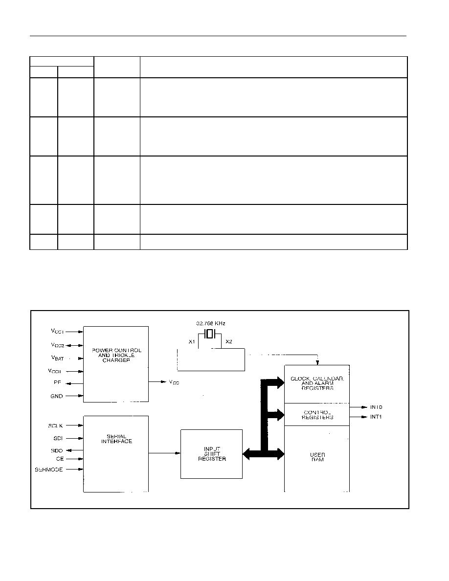
The block diagram in Figure 1 shows the main elements of the serial alarm RTC. The following
paragraphs describe the function of each pin.
Figure 1. BLOCK DIAGRAM
1Hz
OSCILLATOR AND
COUNTDOWN CHAIN
发布紧急采购,3分钟左右您将得到回复。
相关PDF资料
DS1306EN/T&R
IC RTC SERIAL ALARM IND 20-TSSOP
DS1307N
IC RTC SERIAL 512K IND 8-DIP
DS1308U-3+
IC RTC 56BYTE NVRAM I2C 8UMAX
DS1315EN-5/T&R
IC TIME CHIP PHANTOM 20-TSSOP
DS1318E+
IC COUNTER ELAPSED TIME 24-TSSOP
DS1337S+C01
IC RTC SERIAL 2WIRE LP 8-SOIC
DS1338C-33#T&R
IC RTC 56BYTE NV SRAM 16SOIC
DS1339AU+
IC RTC I2C W/ALARM 8USOP
相关代理商/技术参数
DS1305E/TR
制造商:MAXIM 制造商全称:Maxim Integrated Products 功能描述:Serial Alarm Real-Time Clock
DS1305E+
功能描述:实时时钟 Serial Alarm RTC 3-Wire RoHS:否 制造商:Microchip Technology 功能:Clock, Calendar. Alarm RTC 总线接口:I2C 日期格式:DW:DM:M:Y 时间格式:HH:MM:SS RTC 存储容量:64 B 电源电压-最大:5.5 V 电源电压-最小:1.8 V 最大工作温度:+ 85 C 最小工作温度: 安装风格:Through Hole 封装 / 箱体:PDIP-8 封装:Tube
DS1305E+R
制造商:DALLAS 制造商全称:Dallas Semiconductor 功能描述:Serial Alarm Real-Time Clock
DS1305E+T
制造商:DALLAS 制造商全称:Dallas Semiconductor 功能描述:Serial Alarm Real-Time Clock
DS1305E+T&R
制造商:Maxim Integrated Products 功能描述: 制造商:Maxim Integrated Products 功能描述:REAL TIME CLOCK SERL 96BYTE 20TSSOP - Tape and Reel 制造商:Maxim Integrated Products 功能描述:SERIAL ALARMRTC 20PTSSOPT&R LFREE 制造商:Maxim Integrated Products 功能描述:IC RTC SERIAL ALARM 20-TSSOP 制造商:Maxim Integrated Products 功能描述:Real Time Clock Serial Alarm RTC 3-Wire
DS1305E+T&R
功能描述:实时时钟 Serial Alarm RTC 3-Wire RoHS:否 制造商:Microchip Technology 功能:Clock, Calendar. Alarm RTC 总线接口:I2C 日期格式:DW:DM:M:Y 时间格式:HH:MM:SS RTC 存储容量:64 B 电源电压-最大:5.5 V 电源电压-最小:1.8 V 最大工作温度:+ 85 C 最小工作温度: 安装风格:Through Hole 封装 / 箱体:PDIP-8 封装:Tube
DS1305E+TR
制造商:MAXIM 制造商全称:Maxim Integrated Products 功能描述:Serial Alarm Real-Time Clock
DS1305EN
功能描述:实时时钟 Serial Alarm RTC 3-Wire RoHS:否 制造商:Microchip Technology 功能:Clock, Calendar. Alarm RTC 总线接口:I2C 日期格式:DW:DM:M:Y 时间格式:HH:MM:SS RTC 存储容量:64 B 电源电压-最大:5.5 V 电源电压-最小:1.8 V 最大工作温度:+ 85 C 最小工作温度: 安装风格:Through Hole 封装 / 箱体:PDIP-8 封装:Tube